Tech
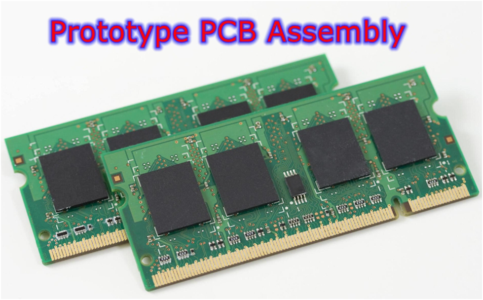
Common Mistakes to Avoid in Prototype PCB Assembly
You may not want to understand that there could be mistakes in the process of making prototype PCB assembly. It first seems a simple concept of assembling parts for a printed circuit board. However, much effort has to go into ensuring this functionality and accuracy; otherwise, it results in a product that can still not be mass-produced.
The prototype should be built up while following all the design specifications so the location on the printed board, soldering, and testing of all the components should be accurate.
It’s critical to avoid errors in PCB assembly prototypes for several reasons:
- Delays and Increased Costs: Any inaccuracies in the prototype assembly process will translate into delays and increased costs. More time will, therefore, have to be spent, and more money shall be spent on remaking or reworking the prototype.
- Easier Corrections in the Early Stages: It is easier to correct early on because the specifications of a design get to be more “locked in” as the device approaches mass production. In other words, changes during this prototype phase are easier to make and are less painful on the budget.
- Faster Development Timeline: If prototype assembly proceeds smoothly, it can speed up the entire development timeline and get a product to market faster.
- Competitive Advantage: Moving through the prototype phase without error can give a business a considerable edge in some markets. You will only win races if you leave the gate quickly.
Common Mistakes
1. Inadequate Planning and Design Review
Take some time to think about the value of detailed planning and careful design review in the process of the PCB assembly prototype. This could be the most timely task, and several issues could be noticed during or after assembly.
Not Thoroughly Reviewing the PCB Design Before the Assembly
- Critical oversight: A quick design review or none at all can lead to layout design blunders. This may result in displaced components or traces, too small a width of the trace, or a lack of space for heat dissipation. This stage is important as it guarantees that DFM is carried out and that all functional requirements are met.
- Consequence of Oversight: By not performing a thorough revision at this stage, simple mistakes can escalate into significant issues that will need rework, costing you a lot of time and money. Therefore, the prototype PCB assembly services are below par.
The Consequences of Overlooking Design Reviews
- Increased Error Rate: Failure to validate the design could result in more assembly errors. Such mistakes often cause rework or, in extreme cases, the need to fully redesign the PCB, which considerably adds to the time and cost of the project.
- Functionality Issues: A concern arises when there is no validation because the design may need to perform as expected. This may lead to functionality issues that can only be detected once the product is already in the development process or even after it has been released to customers.
- Reliability and Safety Concerns: Poor design review may cause an unreliable and unsafe product. In sectors like aerospace, medical devices, or automotive safety, such deficiencies may have a severe impact.

2. Poor Component Selection
The right components serve as a base for your PCB and lead to better prototype PCB assembly services. Thus, this is a critical part of the process of PCB prototype assembly, yet common mistakes result from the need to select the best components.
Using Components that are not Suitable
- Mismatch in functionality: Insufficient knowledge of the nature of the chosen components or how they conform with the application’s requirements may lead to poor performance. For example, if one selects a capacitor with a voltage rating very close to the operating voltage of the circuit, then early failure of the same may result.
- Physical Incompatibility: In some cases, they have even designed the parts so that they cannot fit the PCB layout, therefore making it an unstable design and needing changes that might have been avoided through proper planning at the initial stages of the design.
Ignoring the availability and lead time of components
- Supply Chain Vulnerabilities: Vulnerabilities may be such that they involve component selection. In contrast, the availability of that component in the current market and its lead time could be neglected, halting the project at half of its assembly. On the other hand, a critical IC might take several months of lead time, culminating in a project breakdown.
- Last-Minute Replacements: This situation usually means that the designer has to choose other components that may not be suitable for the circuit, but their presence might be detrimental to PCB performance or increase PCB cost.
3. Ignoring Manufacturer’s Guidelines
The guidelines given by PCB manufacturers must be considered seriously. After all, it is not taken in vain; it is based on the machinery capabilities and processes with which the production of PCBs is carried out effectively.
Overlooking the PCB Manufacturer’s Capabilities and Specifications
- Manufacturer’s Expertise: PCB manufacturers always have very broad guidelines and specifications based on their machinery, processes, and manufacturing abilities. The guidelines are meant to reach out for the best results in producing the PCB.
- Common Oversights: These mistakes are not avoided during the prototype assembly. For example, the design might call out trace widths or hole sizes that are too small for the manufacturer’s equipment to produce, possibly causing assembly problems or even redesigning accurately.
The Impact of Not Following Recommended Design Guidelines
Not adhering to the recommended design guidelines can lead to several detrimental outcomes, including:
- Production Delays: If the design does not meet the required specifications, the designer may have to rework the design or resubmit it for rework. This will result in huge time delays in the prototype assembly.
- Low quality of products and unreliability: In other words, any design pushing the limits further than its producing company capabilities without consultation will result in still higher failure rates of their products. The general quality and reliability of the prototype will be affected, reflecting the quality of the final product.
- Compatibility Issues: Failure to adhere to the guidelines may generate compatibility issues between the listed components and assembly techniques, further complicating the process and finally achieving a non-working prototype.

4. Inadequate Soldering Techniques
Soldering is an essential step during the PCB assembly prototype, with the primary goal of permanently affixing the placed components onto the board. Soldering is one of the significant steps, but most mistakes occur primarily because of the wrong technique or lack of understanding. This can hugely compromise the functionality and reliability of the PCB.
Common Soldering Mistakes and How They Affect PCB Functionality
- Cold joint: Insufficient melting of the solder is one of the common problems. It may lead to an unstable or failed electrical connection due to the weak physical bond formed.
- Overheating: Exposure to too much heat can damage the PCB’s material or affect the circuitry, most commonly resulting in circuit failure.
- Solder Bridges: Excess solder would form bridges between adjacent pads or traces, shorting them and thus causing that area of the circuit to malfunction.
- Insufficient solder: Too little solder will produce very poor or weak joints that could pull apart under stress and will be inadequate to affect a good electrical joint.
These errors, singly or in combination, can compromise the integrity of the PCB, which finally reduces performance or can even cause complete failure of the board.
The Importance of Proper Soldering Temperature and Time
- Temperature Control: The soldering temperature greatly affects the formation of sound, reliable soldered joints. It may prevent the proper flow of solder if it is low; if it is high, damage may occur to the component or the printed circuit board substrate.
- Timing: Timing is an essential factor that needs special care while soldering. Being kept for a long period under high temperatures may burn away the components quickly, whereas, without heat, the solder does not melt to have a good joint.
5. Neglecting Proper Inspection and Testing
Skipping the careful inspection and testing at the assembling stages of a PCB prototype would result in a severe and costly dreadful mistake. These could prove to be detrimental to prototype PCB assembly services.
Skipping Critical Inspections and Testing Phases
- Visual Inspections and Tests: Full visual inspections often don’t catch soldering errors, component misalignments, and many other visible defects if they are not properly carried out.
- Functional Testing: Not conducting functional tests would imply not verifying the prototype against all the operational requirements. This is a crucial step in the verification process, as it checks that all components are doing their function within the circuitry.
- Electrical Testing: Testing with Negligence could include continuity and isolation tests that can produce products where short or open circuits are not detected and may have been manufactured of the design.
However, foregoing these critical inspections and tests risks the failure to notice some defects that would be costly and time-consuming to rectify at later stages.
How Inadequate Testing Can Lead to Failures in the Field
- Undetected Defects: If testing is insufficient, defective products may be released to the market, where, while in actual operation, they are bound to fail. These defects could mean the product is returned, and there are warranty claims and damage to the manufacturer’s reputation.
- Reliability Issues: With long-term testing, these oversights can lead to sufficient earlier failures against perfectly normal operating conditions and consequently affect consumer trust and satisfaction.
- Safety hazards: In cases where the electronic product is part of safety systems, poor testing may lead to catastrophic failures, and users are exposed to serious risks.
6. Overlooking Thermal Management
Thermal management is one of the key areas in the PCB prototype assembly, often highly underrated or understated; however, when enough emphasis is not put on this area, several challenges are occasioned that tend to impair the performance of the PCB. Good thermal management allows the smooth dissipation of heat from the components to avoid overheating and poor operational capacities.
Not Considering Thermal Issues in the PCB Design
- Heat Generation and Buildup: Every electronic component generates heat during work. This can become a critical factor, particularly for high-power components or a densely packed board since the heat generation could be very high due to excessive buildup if there is no proper management.
- Lack of Heat Dissipation Paths: If heat dissipation paths, such as thermal vias or heat sinks, are not designed into it, it will be a problem for heat trapped inside the PCB, and there is a chance of creating hot spots. This can result in hotspots and may be responsible for the component’s integrity and the PCB’s functionality.
The Effects of Poor Thermal Management on PCB Performance
- Reduced Lifespan of Components: Overheating is the easiest way to accelerate the aging of electronic components. It reduces the operational life of such components and eventually leads to premature failure.
- Performance degradation: Most electronic components, like semiconductors, tend to degrade in performance if they are exposed to high temperatures. For example, with increased temperature, the sensors will have a reduced level of accuracy, while the processor and power components’ speed and efficiency increase.
- Thermal Runaway: Poor thermal management can lead to thermal runaway under the most extreme conditions, especially for power components, where an increase in temperature will also increase the current, hence temperature, in a self-feeding cycle that will destroy the component and possibly lead to board or system failure. Reliability Issues: Long-term reliability issues are related to stress from thermal cycling, among others, like cracks of the solder joints, delamination of layers in PCBs, etc.

7. Mismanagement of PCB Layout
The PCB layout is critical to the prototype PCB assembly and directly affects the PCB’s performance, reliability, and manufacturability. Mishandling in this stage makes it difficult to quickly rectify hardware signal integrity problems. Understanding and avoiding common layout mistakes is essential for ensuring the successful function of the PCB.
Common Layout Mistakes
- Trace Width: On the negative side, narrow traces are resistive and hence will become hot, implying that in the long run, it might affect the performance of the PCB. A wide track also wastes precious space on the PCB and makes the board layout difficult.
- Insufficient Spacing: This happens when the space is insufficient to obtain correct spacing between the traces, pads, and components. This defect can even generate a place that can result in short circuits and, at the same time, cause problems in the soldering process with problems of electrical isolation that could affect the operation of the whole circuit.
- Ignoring Power Integrity: A wrong power distribution plan might cause a voltage drop, further causing the instability of the power supply to components and affecting general PCB performance.
Failure to provide a clear return path for the signal: One of the most common, careless mistakes leading to problems with EMI is poor signal integrity, from the circuit not working.
The Significance of Layout in Signal Integrity and Functionality
- Signal Integrity: High-speed designs require sensible PCB layouts, as signal integrity is usually needed. The layout methodology of differential pairing and loop area minimization will bring most of the signal degradations and EMI under control. It then directly reflects on how PCBs work, all the components being placed correctly and with accurate connection. Hence giving way to effective power distribution.
- Functionality: The layout directly impacts the PCB’s functioning since it ensures that all components are correctly located and connected, that power is distributed equally, and that thermal management is considered. A well-designed layout can also make circuit testing and troubleshooting more efficient and enhance the PCB prototype assembly.
Conclusion
Prototype PCB assembly is an inflection stage of all developmental stages of electronic devices. Paying attention to the details and best practices can positively reflect on the product’s success in the field. The most common mistakes that should not be committed include the following:
- Poor planning.
- Wrong choice of components to be used.
- Ignoring the manufacturer’s guidelines, techniques for soldering, and proper inspection and testing.
- Thermal management.
- Mismanagement of PCB layout.
This would cause expensive mistakes, lengthen the development timelines, and compromise the functionality and reliability of the device.
The best prototype manufacturers should be proficient and experienced in their paramount role. The requirements that some of the best prototype manufacturers must meet are the following:
- Advanced Manufacturing Capabilities: Leverage high-tech technology in manufacturing and testing prototypes per sound methodologies.
- DFM (Design for Manufacturability) Expertise: DFM (Design for Manufacturability) offers insights into product and part design, enabling one to optimize designs and reduce
- Processes of Quality Assurance: A set of checks, including inspection and tests, ensures that the prototype meets every requirement and performance criterion.
- Supply Chain Management: Assist in selecting and procuring components and managing the supply chain difficulties within the timeline to keep the project going.
This is greatly leveraged with the choice of a manufacturing partner that is critical in their competency, ability, and commitment to quality. These have huge leverage in prototype development, where potential problems are identified and corrected early. Help far more than simple collaboration from concept to market. It lays down the foundation of success and life far into the foreseeable future of the device. That means, in the future, the strategic investment is contracting with reputable and experienced manufacturers for every project related to electronic devices.

How Policy Charges Affect Your Returns Over the Long Term
5 Best Cloud Phone in 2026 for Mobile Account Operations

Laser Drilled Microvia Technology: Design Principles for Reliable HDI PCB Manufacturing

How Long Do Samsung Phones Last? Lifespan, Software Updates, and the Right Time to Upgrade

Godrej Washing Machines in 2026: Types, Prices, and What to Know Before Buying

TrendyTech’s Data Engineer Training: Build Skills for a Successful Career

Why FastTurnPCBs Matters for High-Frequency PCB Projects

CurlyMe Hair Half Wigs & Crochet Hair For Summer Protective Style
5 Simple CNC Tooling Choices That Improve Shop Efficiency
How Trading Apps Are Shaping the Future of Retail Investing
CurlyMe Hair Half Wigs & Crochet Hair For Summer Protective Style
5 Simple CNC Tooling Choices That Improve Shop Efficiency
How Trading Apps Are Shaping the Future of Retail Investing

Migrating from Prometheus to VictoriaMetrics: A Step-by-Step Guide
TrendyTech’s Data Engineer Training: Build Skills for a Successful Career
Why FastTurnPCBs Matters for High-Frequency PCB Projects
Godrej Washing Machines in 2026: Types, Prices, and What to Know Before Buying
How Long Do Samsung Phones Last? Lifespan, Software Updates, and the Right Time to Upgrade
Laser Drilled Microvia Technology: Design Principles for Reliable HDI PCB Manufacturing
5 Best Cloud Phone in 2026 for Mobile Account Operations


 Tech2 years ago
How to Use a Temporary Number for WhatsApp
- Business2 years ago
Sepatuindonesia.com | Best Online Store in Indonesia
- Social Media2 years ago
The Best Methods to Download TikTok Videos Using SnapTik
- Technology2 years ago
Top High Paying Affiliate Programs
- Tech1 year ago
Understanding thejavasea.me Leaks Aio-TLP: A Comprehensive Guide
- FOOD2 years ago
How to Identify Pure Desi Ghee? Ultimate Guidelines for Purchasing Authentic Ghee Online

 Instagram4 years ago
Free Instagram Auto Follower Without Login
- Instagram4 years ago
Free Instagram Follower Without Login