Technology
Laser Drilled Microvia Technology: Design Principles for Reliable HDI PCB Manufacturing

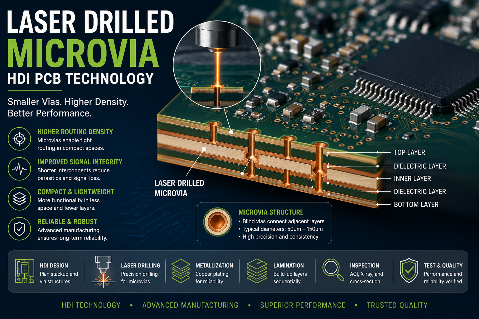
Electronic devices continue to shrink while delivering increasingly sophisticated functionality. Modern products often require higher component density, faster signal transmission, and improved electrical performance within significantly smaller form factors. Conventional through hole PCB technology is frequently unable to meet these requirements, leading engineers to adopt High Density Interconnect (HDI) designs that use laser drilled microvias to achieve greater routing density and more efficient layer interconnections.
A properly designed laser drilled microvia structure enables shorter electrical paths, improved signal integrity, higher routing efficiency, and compact multilayer PCB layouts. However, successful implementation requires careful attention to stackup planning, via structures, material selection, manufacturing tolerances, and Design for Manufacturability (DFM).
This guide explains the engineering principles behind laser drilled microvia technology and the considerations that help improve reliability throughout PCB fabrication and assembly.
What Are Laser Drilled Microvias?
Microvias are very small blind vias created using precision laser drilling rather than conventional mechanical drilling.
Unlike plated through holes that extend through the entire PCB, microvias typically connect adjacent layers, making them ideal for HDI circuit designs where routing space is limited.
Laser drilled microvias are commonly used to:
- Connect high density components
- Escape fine pitch BGAs
- Increase routing density
- Reduce signal path length
- Improve layer utilisation
- Support compact PCB layouts
Because of their small dimensions, laser drilling provides significantly greater placement flexibility than traditional mechanical drilling methods.
Why HDI Designs Use Microvias
As component packages continue to become smaller, PCB routing becomes increasingly challenging.
Microvias allow engineers to route signals efficiently beneath fine pitch devices while preserving valuable routing channels on other layers.
Advantages include:
- Higher routing density
- Smaller PCB dimensions
- Reduced layer count in some applications
- Improved signal integrity
- Lower parasitic inductance
- Better high speed performance
- Greater design flexibility
These characteristics make laser drilled microvias particularly valuable for telecommunications, medical devices, industrial electronics, automotive systems, and consumer products.
Understanding Microvia Structures
Different HDI applications require different microvia configurations depending on routing complexity and layer count.
Common structures include:
- Blind microvias
- Staggered microvias
- Stacked microvias
- Skip vias
- Sequential build up structures
Each configuration offers unique advantages depending on signal routing, manufacturing capability, and reliability requirements.
Selecting an appropriate via structure should always be based on both electrical and manufacturing considerations.
Stackup Planning Before Layout
Microvia implementation begins with proper PCB stackup development.
The stackup determines:
- Layer count
- Dielectric thickness
- Copper distribution
- Sequential lamination requirements
- Controlled impedance
- Routing strategy
Changing the stackup after PCB routing often requires substantial redesign.
Engineers should therefore complete stackup planning before detailed layout begins.
Manufacturing capabilities should also be reviewed to ensure the proposed HDI construction can be fabricated consistently.
Material Selection
Material selection influences both electrical performance and manufacturing reliability.
Engineers should evaluate:
- Dielectric materials
- Glass transition temperature
- Resin flow characteristics
- Copper weight
- Thermal expansion
- Surface finish compatibility
Selecting materials appropriate for HDI fabrication helps maintain dimensional stability throughout multiple lamination cycles while supporting reliable microvia performance.
Material compatibility should always be confirmed before prototype release.
Routing Around Fine Pitch Components
Microvias are frequently used to route signals beneath advanced component packages where mechanical vias cannot be accommodated.
When routing around fine pitch devices, designers should consider:
- Escape routing strategy
- Via placement
- Copper balancing
- Controlled impedance
- Signal layer transitions
- Return current paths
Well planned routing reduces congestion while improving electrical performance throughout the PCB.
Design for Manufacturability Review
Every HDI PCB incorporating laser drilled microvias should undergo a detailed Design for Manufacturability review.
Typical review areas include:
- Stackup verification
- Via structures
- Copper balancing
- Registration tolerances
- Sequential lamination
- Controlled impedance
- Fabrication capability
- Manufacturing tolerances
Completing DFM before fabrication helps identify potential manufacturing challenges while reducing prototype revisions.
Engineering Design Checklist
Before releasing an HDI PCB containing laser drilled microvias for fabrication, engineering teams should confirm that all major design activities have been completed.
| Design Area | Verification |
| Stackup | Finalised before routing |
| Microvia structure | Selected for application |
| Material selection | Confirmed |
| Routing strategy | Reviewed |
| Controlled impedance | Verified |
| DFM review | Completed |
| Manufacturing documentation | Approved |
| Fabrication capability | Confirmed |
Using a structured engineering review process helps improve manufacturability while reducing development risk.
Laser Drilling and Manufacturing Considerations
Producing reliable microvias requires highly controlled manufacturing processes. Unlike conventional mechanical drilling, laser drilling creates extremely small via openings that must be accurately positioned before plating and subsequent lamination processes.
Manufacturing considerations typically include:
- Laser drilling accuracy
- Registration control
- Hole quality
- Copper plating consistency
- Resin removal
- Sequential lamination
- Surface preparation
Maintaining tight process control throughout these stages helps ensure consistent electrical performance while reducing the likelihood of manufacturing defects.
Because HDI boards often involve multiple build-up cycles, close coordination between design and fabrication teams is essential before production begins.
Inspection and Quality Assurance
Many microvia features are embedded within the PCB after lamination, making comprehensive inspection an essential part of the manufacturing process.
Quality verification generally occurs at several stages rather than relying solely on final inspection.
Typical inspection methods include:
- Automated Optical Inspection (AOI)
- X ray inspection
- Cross section analysis
- Electrical continuity testing
- Layer registration verification
- Copper plating inspection
- Visual examination of external features
These inspections help verify plating integrity, microvia quality, layer alignment, and manufacturing consistency before boards move to assembly.
Reliability Testing
HDI PCBs containing laser drilled microvias are often used in products that operate under demanding electrical and environmental conditions.
Reliability testing helps confirm that the completed PCB performs consistently throughout its expected service life.
Common evaluations include:
- Thermal cycling
- Electrical continuity verification
- Environmental exposure testing
- Mechanical stress testing
- High temperature storage
- Insulation resistance testing
The specific testing programme depends on the application, operating environment, and applicable industry standards.
Planning reliability validation during the design phase helps ensure that testing requirements are incorporated into the development schedule.
Preparing for Production
A successful engineering prototype should demonstrate not only functional performance but also manufacturing readiness.
Before moving to production, engineering teams should review:
- Manufacturing documentation
- Material availability
- Process repeatability
- Inspection procedures
- Testing requirements
- Revision control
- Production scalability
Evaluating these factors during prototype development reduces engineering changes while improving manufacturing efficiency as production volumes increase.
Common Microvia Design Mistakes
Many HDI design challenges arise during early layout planning rather than during fabrication.
Frequently encountered issues include:
- Changing the PCB stackup after routing
- Selecting inappropriate microvia structures
- Poor copper balancing
- Inadequate Design for Manufacturability review
- Ignoring manufacturing capability limitations
- Incomplete fabrication documentation
- Insufficient inspection planning
Avoiding these issues early helps improve manufacturing consistency while reducing prototype iterations and project delays.
Engineering Release Checklist
Before releasing an HDI PCB incorporating laser drilled microvias for fabrication, engineering teams should confirm that all critical design activities have been completed.
| Review Area | Verification |
| PCB stackup | Approved before routing |
| Microvia structure | Verified |
| Material selection | Confirmed |
| Manufacturing capability | Reviewed |
| DFM review | Completed |
| Inspection requirements | Defined |
| Reliability testing | Planned |
| Manufacturing documentation | Complete |
| Revision control | Updated |
A structured release process improves communication between engineering, procurement, and manufacturing teams while reducing development risks.
Future Design Improvements
Prototype evaluation often reveals opportunities to further optimise HDI designs before production.
Engineering teams should document:
- Manufacturing observations
- Inspection results
- Electrical performance
- Thermal behaviour
- Reliability testing outcomes
- Routing improvements
- Material recommendations
Capturing engineering feedback after each prototype iteration supports continuous improvement while helping future revisions progress more efficiently.
Final Thoughts
Laser drilled microvia technology has become a fundamental element of modern HDI PCB design, enabling engineers to achieve higher routing density, improved signal integrity, and more compact electronic products. However, reliable results depend on far more than simply selecting microvias during PCB layout. Successful projects require careful stackup development, appropriate material selection, controlled manufacturing processes, comprehensive inspection, and thorough reliability validation.
Treating microvia implementation as a complete engineering process helps reduce prototype revisions, improve manufacturing consistency, and support a smoother transition into production. Early collaboration between PCB designers and manufacturing specialists remains one of the most effective ways to minimise development risks while optimising fabrication efficiency.
For organisations selecting an experienced HDI PCB manufacturer, it is important to evaluate engineering expertise, HDI manufacturing capabilities, inspection methods, and quality management systems alongside production capacity and lead times. Manufacturing processes, achievable turnaround times, and recommended HDI structures should always be confirmed after reviewing the specific PCB design, application requirements, and production objectives.
By following established engineering best practices throughout design, fabrication, and validation, development teams can successfully implement laser drilled microvia technology to create compact, high performance, and highly reliable HDI printed circuit boards.


Type-C to C vs Type A to Type C Cable: What’s the Difference?

How Executive Search Software Selects and Manages Senior Leadership Candidates

Data Science Course in Pune with Placement Support: From Classroom Training to Your First Job

Ethical Hacking Courses in Mumbai with Placement: Institutes, Duration, Fees & Jobs 2026

Best Micro Influencer Agency Singapore: Why Micro Beats Macro for Conversion

What Makes a Crypto Exchange Top-Rated? Understanding the Ranking Criteria
Why These Data Science Institutes in Delhi Are Preferred by Top Tech Recruiters?

How Long Does It Take to Register a Company in USA?

TeraBox Mod APK: Exploring Cloud Storage and File Management on Android

Future of Management Accounting: Why CMA Certification Skills Are in High Demand
How Long Does It Take to Register a Company in USA?
Data Science Course in Pune with Placement Support: From Classroom Training to Your First Job
TeraBox Mod APK: Exploring Cloud Storage and File Management on Android
Ethical Hacking Courses in Mumbai with Placement: Institutes, Duration, Fees & Jobs 2026
Best Micro Influencer Agency Singapore: Why Micro Beats Macro for Conversion
Future of Management Accounting: Why CMA Certification Skills Are in High Demand
What Makes a Crypto Exchange Top-Rated? Understanding the Ranking Criteria
Why These Data Science Institutes in Delhi Are Preferred by Top Tech Recruiters?
How Executive Search Software Selects and Manages Senior Leadership Candidates
Type-C to C vs Type A to Type C Cable: What’s the Difference?


 Tech2 years ago
How to Use a Temporary Number for WhatsApp
- Business3 years ago
Sepatuindonesia.com | Best Online Store in Indonesia
- Social Media2 years ago
The Best Methods to Download TikTok Videos Using SnapTik
- Technology2 years ago
Top High Paying Affiliate Programs
- Tech2 years ago
Understanding thejavasea.me Leaks Aio-TLP: A Comprehensive Guide
- FOOD2 years ago
How to Identify Pure Desi Ghee? Ultimate Guidelines for Purchasing Authentic Ghee Online

 Instagram4 years ago
Free Instagram Auto Follower Without Login
- Instagram4 years ago
Free Instagram Follower Without Login